Lead Compensators
I have been studying the basics of control theory in preparation for the Mechanical Engineering qualifying exams coming this fall. I want to write a series of posts that will help me consolidate what I am learning and practice explaining it to others. There is a lot of material to cover, but some of the topics that I am most concerned about are related to designing dynamic compensators and controllers. Today, I am going to review lead compensation.
First, I should note that I understand the terms “compensation” and “controller” to be interchangeable [1], although I will follow the literature convention which differentiates between lead and lag compensators and PD and PI controllers [2]. Regardless, a lead compensator and a PD controller perform similar functions because they both add phase lead to a system [2]. The primary reason to use a lead compensator is to add damping to the system.
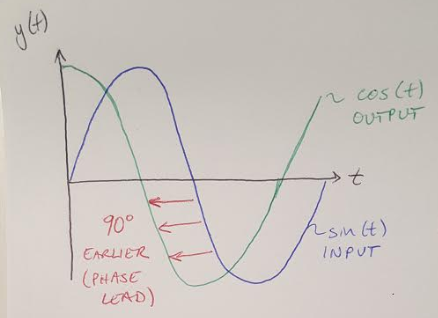
Figure 1
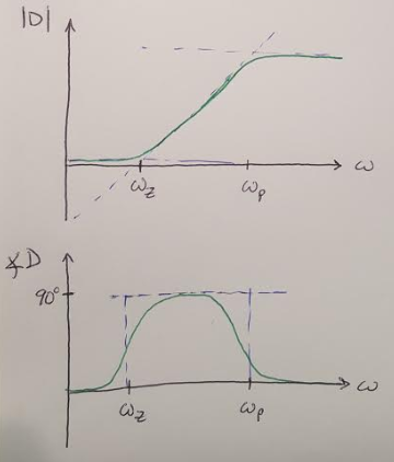
Phase lead means that the output of the system leads the input of the function by a given phase shift [3]. Figure 1 shows what that looks like in the time domain [3]. A lead compensator is designed to add phase to a system within a given range of frequencies (as compared to a PD controller, which also adds phase, but the phase is added at every frequency above the breakpoint frequency of the controller zero) [2]. Figure 2 shows what the phase addition looks like in the frequency domain (i.e. on a Bode magnitude and phase plot) [2].
Figure 2
Why would we need to add phase lead to a system? Designers typically need to meet 3 types of design requirements [2]:
- Crossover frequency - determines the closed loop bandwidth, rise time and settling time
- Phase margin - determines damping and overshoot
- Low frequency gain - determines steady state error
We can use a lead compensator to meet Requirement #1, the crossover frequency, by selecting a suitable gain for the compensator. The lead compensator is particularly well suited to adjusting the plant’s phase margin (Requirement #2) because we can use it to increase the phase margin by adding phase lead. And again, our choice of gain will determine the steady state error of the system (Requirement #3). We should note that a lead compensator will increase the gain at high frequency (see Figure 2) but the increase is constant above the second corner frequency, so it applies less noise amplification than we would see if we added a pure zero to the system [3].
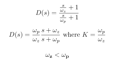
Speaking of adding poles and zeros, what is the transfer function for a lead compensator? I have written it in two different forms below [3].
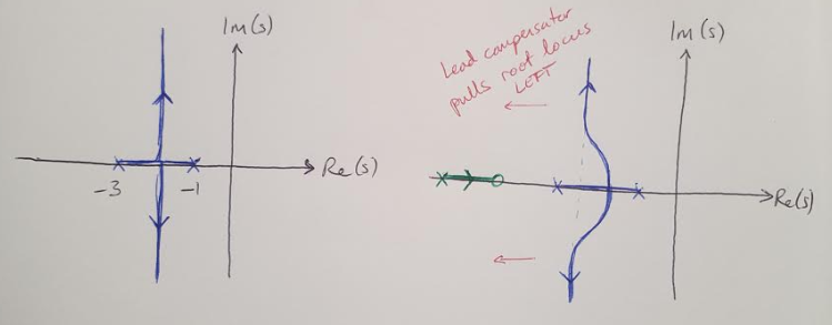
The important thing to note here is that the pole must be at a higher frequency (i.e. it must be faster) than the zero for a lead compensator. (The reverse order of pole and zero frequency will result in a lag compensator, more on this later.) And if you are a fan of the root locus plot, I have drawn the root locus for a system before and after the addition of a lead compensator to show its impact on the closed loop system in Figure 3 [2].
Figure 3
Notice that we place the pole and zero of the lead compensator to the left of the plant poles and zeros. In other words, we make the compensator faster so that the slower plant poles and zeros still dominate the behavior of the system [2]. A good rule of thumb is to put the zero near the closed loop natural frequency, and to put the pole 5 to 20X away from the zero [2]. We do not want to make the lead compensator too fast, however, because this will amplify high frequency noise.
Generally speaking, a lead compensator will contribute about 70 degrees to the phase margin [2]. If more phase is required, a double lead compensator can be used [2]. This compensator simply has 2 poles in the same location and 2 zeros in the same location.
The general design process for designing a lead compensator is as follows. Note that an alternate expression for the compensator is used in this design process as stated in this equation [2]:
Design process [2]:
- Check system type if you have a steady state error requirement using Final Value Theorem. Add a pole as necessary to get finite steady state error. [4]
- Determine the open loop gain required to meet the steady state error and bandwidth requirements. Use Final Value Theorem to solve for the gain K. [4]
- Evaluate the phase margin of the system with this gain.
- Find the max phase that the lead compensator needs to add to the system by comparing the current phase margin with the desired phase margin and adding 10 degrees.
- Find the ratio, alpha, between the zero and pole frequencies using the equation:
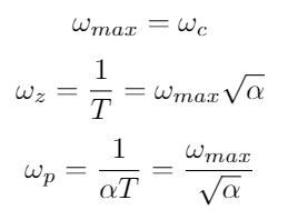
- Calculate the zero and pole frequencies using the following equations:
- Check the phase margin again to see if it meets the design specification.
- Iterate on the design until the specifications are met.
References
[1] Douglas, Brian. “What are Lead Lag Compensators? An Introduction.” https://www.youtube.com/watch?v=xLhvil5sDcU&list=PLUMWjy5jgHK1NC52DXXrriwihVrYZKqjk&index=33 Visited on 6/14/2019.
[2] Franklin, G., Powell, J.D., Emami-Naeini, A. Feedback Control of Dynamic Systems, 6th ed. Pearson. 2009.
[3] Douglas, Brian. “Designing a Lead Compensator with Root Locus.” https://www.youtube.com/watch?v=NMpmb0ihoFo&list=PLUMWjy5jgHK1NC52DXXrriwihVrYZKqjk&index=34 Visited on 6/14/2019.
[4] Douglas, Brian. “Designing a Lead Compensator with Bode Plot.” https://www.youtube.com/watch?v=rH44ttR3G4Q&list=PLUMWjy5jgHK1NC52DXXrriwihVrYZKqjk&index=35 Visited on 6/17/2019.

