Designing Lead and Lag-Lead Compensators with Bode Plots
We are pretty much down to the wire (the qual is tomorrow) so I just want to write a couple notes on how to design lead and lag compensators with Bode plots. All of the information presented here comes from Nise [1].
I’ve talked before about why we use Bode plots versus Nyquist plots versus root locus plots before, and I just wanted to add a thought to that post here. Nise argues that there is an additional advantage to using Bode plots over the root locus for design: we can implement a steady state requirement and then proceed to design the transient response. The root locus does not encode any information about the steady state requirement so that’s why Bode plots are more useful for designing to that type of specification.
We are going to talk about designing both lead and lag compensators here. One key difference between the design approaches for the two compensators is that for lag compensators, we are going to try to have a minimal impact on the phase diagram, because we are trying NOT to affect the steady state response. Lag compensators are intended for improving steady state response - in other words, we are focused on tuning the DC gain in the magnitude plot. Conversely, lead compensators are trying to meet transient performance specifications, which means that they need to change the phase diagram to add phase margin. Lead compensator design is also focused on modifying the gain crossover frequency so that it has the proper response.
Lag Compensators
I have already posted about lag compensators but I just wanted to add a note that the general equation for them is the following:

Note that alpha is greater than 1 for this expression (this ensures the pole is closer to the Imaginary axis than the zero).
Lead Compensators
In the figure below I have shown the behavior of a lead compensator on a Bode plot, as well as demonstrated how it modifies the uncompensated system.
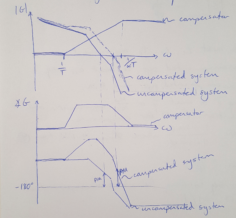 Figure 1
The general equation for a lead compensator is as follows, noting that beta is less than 1:

Nise offers a general design approach for lead compensators which goes as follows:
(1) Calculate the required bandwidth to meet the transient performance requirement (usually expressed in terms of the settling time, rise time or peak time). We use the following equation to obtain the bandwidth.

(2) Set the DC gain of the uncompensated system to meet the steady state requirements (this requires use of the Final Value Theorem).
(3) Draw the Bode plot for the uncompensated system and obtain the current phase margin available.
(4) Calculate the phase margin required to meet the damping coefficient or percent overshoot requirement. Don’t forget to add some extra phase margin to compensate for imperfections in the controller design (approximately 10 degrees of phase is good).
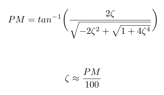
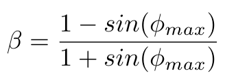
(5) Calculate the value of beta from the following equation. Use the phase margin obtained in Step (4) as the maximum phase value:
(6) Calculate the gain corresponding to the maximum phase frequency using the equation below. We are going to look for the new phase margin frequency that we want to design for by looking for places where this gain is present on the Bode plot.
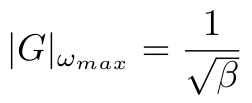
(7) Find the new maximum phase margin frequency by looking for the point where the uncompensated system’s magnitude curve is the negative value of the gain calculated in Step (6).
(8) Select the break frequencies, T and beta*T using the maximum frequency equation given below:
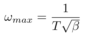
(9) Reset the system gain to adjust for the compensator’s gain.
(10) Check that the bandwidth still meets design requirements. Simulate the system and repeat the design as necessary.
Please check my next post for a worked example of a lead compensator design problem.
Lag-Lead Compensators
The lag-lead compensator is the analog to the PID controller. The lag-lead compensator can meet multiple design requirements: the lag component reduces high frequency gain, stabilizes the system and meets steady state requirements, while the lead component is used to meet transient response design requirements. The general equation for this kind of compensator is given below:

Notice that the equation uses one parameter, gamma, to set the locations of the poles and zeros for both the lead and lag parts of the compensator. This is because Nise wanted to show how to design a single, passive lag-lead network, which requires tying the entire design into this one parameter, gamma. Please note that it is also possible to design a lag-lead compensator with completely unrelated pole and zero locations.
As before, Nise presents a general design procedure for lag-lead compensators as follows:
(1) Calculate the required bandwidth to meet the transient performance requirement (usually expressed in terms of the settling time, rise time or peak time). Use the equation provided above.
(2) Set the DC gain of the uncompensated system to meet the steady state requirements (this requires use of the Final Value Theorem).
(3) Draw the Bode plot for the uncompensated system and obtain the current phase margin available.
(4) Calculate the phase margin required to meet the damping coefficient or percent overshoot requirement. Don’t forget to add some extra phase margin to compensate for imperfections in the controller design (approximately 10 degrees of phase is good).
(5) Select a new phase margin frequency that is slightly less than the bandwidth.
(6) At this new phase margin frequency, calculate the phase lead required to obtained the phase margin from Step (4). Add some additional phase to adjust for the lag compensator’s effects, if you have not already done so in Step (4).
(7) Design the lag compensator. Choose the higher breakpoint frequency as the phase margin frequency divided by 10. Nise uses a plot of the interaction between beta and the phase margin to select beta, but for our purposes, I think that spacing the pole and zero of the lag compensator apart by a factor of 10 is sufficient for our design purposes.
(8) We can calculate gamma as the inverse of beta, so now we are ready to design the lead compensator. Use the equation given below to find T.
(9) Check that the bandwidth still meets design requirements. Simulate the system and repeat the design as necessary.
In another post I will show a worked example for this type of problem.
References:
[1] Nise, Norman S. Control Systems Engineering, 4th Ed. John Wiley & Sons, Inc. 2004.
